Author Affiliations
Abstract
1 School of Physics, State Key Laboratory of Crystal Materials, Shandong University, Jinan 250100, China
2 Collaborative Innovation Center of Light Manipulations and Applications, Shandong Normal University, Jinan 250358, China
3 Key Laboratory of Materials for High-Power Laser, Shanghai Institute of Optics and Fine Mechanics, Chinese Academy of Sciences, Shanghai 201800, China
4 Department of Physics, Center for Ion Beam Application and Center for Electron Microscopy, Wuhan University, Wuhan 430072, China
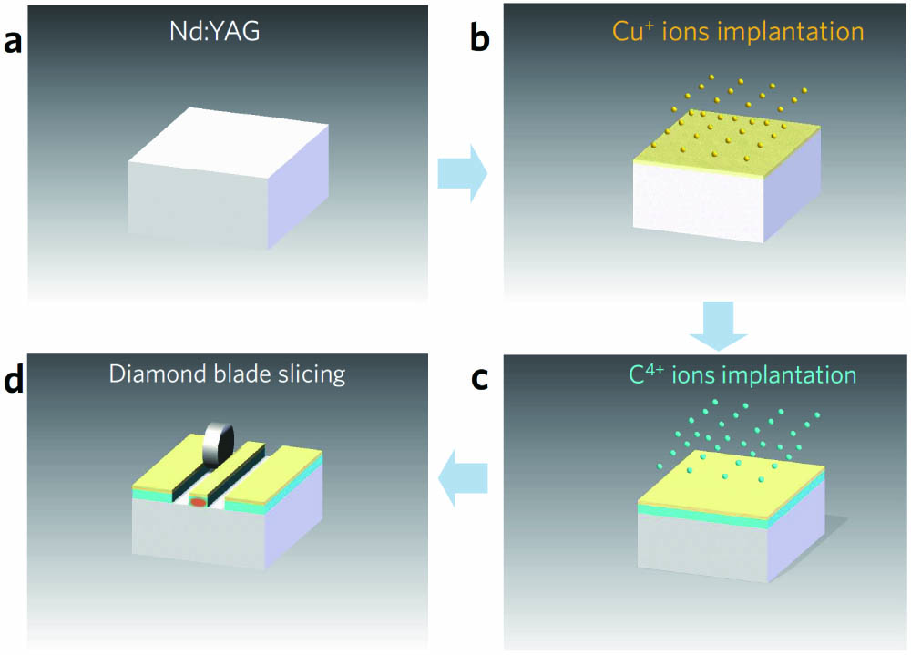
Copper (Cu) nanoparticles (NPs) are synthesized under the near-surface region of the (Nd:YAG) crystal by direct ions implantation. Subsequently, the monolithic ridge waveguide with embedded Cu NPs is fabricated by ions irradiation and diamond saw dicing. The nonlinear optical response of the sample is investigated by the Z-scan technique, and pronounced saturable absorption is observed at the 1030 nm femtosecond laser. Based on the obvious saturable absorption of Cu NPs embedded Nd:YAG crystal, 1 μm monolithic mode-locked pulsed waveguide laser is implemented by evanescent field interaction between NPs and waveguide modes, reaching the pulse duration of 24.8 ps and repetition rate of 7.8 GHz. The work combines waveguides with NPs, achieving pulsed laser devices based on monolithic waveguide chips.
waveguide lasers nanoparticles localized surface plasmon resonance saturable absorption Chinese Optics Letters
2021, 19(2): 021301
Author Affiliations
Abstract
1 School of Physics, State Key Laboratory of Crystal Materials, Shandong University, Jinan 250100, China
2 State Key Laboratory of Crystal Materials and Institute of Crystal Materials, Shandong University, Jinan 250100, China
Graphene and other extraordinary two-dimensional materials together with recent advances in optical modulators have set the foundations for the widespread applications of next-generation optoelectronic devices. In this work, we report on the high-performance fundamentally mode-locked waveguide laser modulated by chemical-vapor-deposition-grown WSe2 as a saturable absorber. By incorporating a WSe2 sample into a monolithic Nd:YVO4 waveguide platform, 6.526 GHz picosecond pulsed laser generation has been achieved at the wavelength of 1 μm with pulse duration of 47 ps.
160.4236 Nanomaterials 140.4050 Mode-locked lasers 140.3540 Lasers, Q-switched Chinese Optics Letters
2019, 17(2): 020013
贵州大学材料与冶金学院, 贵州 贵阳 550003
采用共沉淀法合成钇铝石榴石(YAG)纳米粉体,经干压成型后进行宽带激光烧结,获得YAG透明陶瓷。利用X射线衍射(XRD)、扫描电镜(SEM)对YAG粉体及陶瓷进行表征,研究结果表明,前驱体经1100 ℃焙烧2 h后获得了纯相YAG粉体,粉体近似球形,平均颗粒尺寸约为50 nm;宽带激光烧结后可得到相对密度为99%的YAG透明陶瓷,在可见光区域最大透射率达到32%。
光学制造 透明陶瓷 共沉淀法 宽带激光烧结 钇铝石榴石


